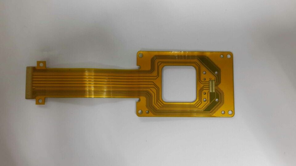
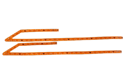
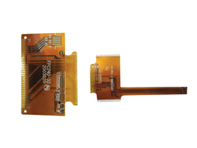
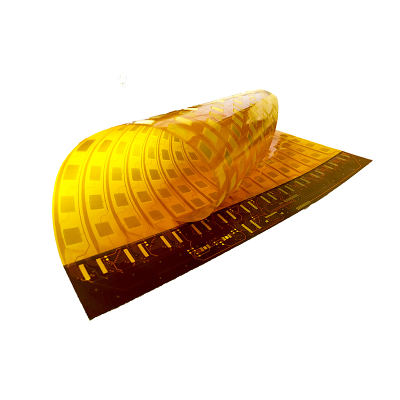
PCB type: FPC flexible circuit board
Number of layers: 8R 2F layers
Thickness of PCB: 1.2mm
Surface treatment: Electroless gold plating
Minimum trace width/spacing: 5/6mil
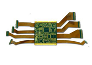
Introduction to 10-layer rigid-flex FPC HDI boards
Basic concepts
The 10-layer rigid-flex FPC HDI board combines the characteristics of the rigid-flex printed circuit board (FPC) and the high-density interconnect (HDI) board. The rigid-flex printed circuit board is formed by combining flexible printed circuit boards and rigid printed circuit boards through processes such as pressing according to relevant process requirements, and it has the characteristics of both FPC and PCB. The HDI board is characterized by high density, with more densely arranged circuits and vias, enabling higher wiring density and smaller size.
Application fields
Mobile phone field
It is widely used in mobile phones, such as the folding parts of foldable mobile phones, camera modules, keyboards, radio frequency modules, etc. These parts need to have the ability of bendability and high-density wiring, and the 10-layer rigid-flex FPC HDI board exactly meets these requirements.
Industrial use
It covers aspects such as industry, military, and medical care. Industrial parts usually have high requirements for precision, safety, and durability. The 10 – layer rigid – flex FPC HDI board can provide high reliability, low impedance loss, complete signal transmission quality, and durability. However, due to its complex manufacturing process, the production volume is relatively small and the unit price is relatively high.
Automobile field
It is commonly used for various connections inside vehicles, such as connecting the buttons on the steering wheel to the main board, the connection between the screen of the vehicle video system and the control panel, the operation connection of audio or function keys on the side doors, the sensors of the reversing radar image system (including those for air quality, temperature and humidity, special gas adjustment, etc.), the vehicle communication system, satellite navigation, the connection board between the rear – seat control panel and the front – end controller, and the vehicle external detection system. These application scenarios require the circuit board to adapt to the complex in – vehicle environment and be able to achieve reliable signal transmission.
Consumer electronics
It is also used in consumer products such as digital still cameras (DSC) and digital video cameras (DV). In terms of performance, it can achieve three – dimensional connections between different rigid PCBs and components. At the same line density, it can increase the total usable area of the PCB, improve the circuit carrying capacity, and reduce the signal transmission limit of contacts and the assembly error rate. In terms of structure, its features of being thin, light and capable of flexible wiring help to reduce the volume and weight of products.
Production difficulties
Interlayer alignment accuracy
Since the circuit board has a relatively large number of layers and the customer has strict requirements for the alignment of each layer, the tolerance for inter – layer alignment is usually controlled within ±75μm. However, considering factors such as the large design of the unit size, the temperature and humidity in the pattern transfer workshop, the misalignment superposition caused by the inconsistent expansion and contraction of different core board layers, and the inter – layer positioning method, it makes the control of inter – layer alignment more difficult.
Inner layer circuit production
The use of special materials such as high-TG, high-speed, high-frequency, thick copper, and thin dielectric layers has put forward higher requirements for the production of inner-layer circuits and the control of graphic dimensions. For example, it is necessary to ensure the integrity of impedance signal transmission. In addition, small line widths and line spacings will lead to an increase in open and short circuits, an increase in micro-shorts, and a decrease in the qualified rate. A large number of signal layers in fine circuits will increase the probability of missed detections in the inner-layer automatic optical inspection (AOI). The inner-layer core board is relatively thin, prone to wrinkling, resulting in poor exposure, and is likely to curl during the etching process. Moreover, most 10-layer boards are system boards with relatively large unit sizes, and the cost of scrapping finished products is relatively high.
Lamination production
When multiple inner core boards and prepregs are stacked and pressed during production, defects such as sliding boards, delamination, resin voids, and residual bubbles are likely to occur. When designing the laminated structure, it is necessary to fully consider the heat resistance, voltage resistance, resin filling amount, and dielectric thickness of the materials, and set a reasonable pressing program. At the same time, a large number of layers will make it difficult to keep the expansion and contraction control and dimensional coefficient compensation consistent. A thin inter – layer insulation layer can also easily lead to the failure of the inter – layer reliability test.
Drilling production
The use of special boards such as those with high TG, high speed, high frequency and thick copper has increased the difficulty of drilling roughness, drilling burrs and desmearing.
Key production process control
Material selection
With the development of electronic components towards miniaturization and multi – functionality, there are lower requirements for the dielectric constant and dielectric loss of electronic circuit materials. At the same time, low CTE (coefficient of thermal expansion), low water absorption rate and better copper – clad laminate materials are needed to meet the processing and reliability requirements. For high – layer thick – copper circuit boards, prepregs with high resin content should be selected to ensure that the resin flow of the inter – layer prepregs is sufficient to fill the inner – layer patterns. The thickness of the insulating dielectric layer needs to be strictly controlled. If it is too thick, the finished board is likely to be overly thick; if it is too thin, quality problems such as dielectric delamination and failure in high – voltage testing may occur.
Lamination structure design
In the design of the laminated structure, factors such as the heat resistance, voltage resistance, glue filling amount of the materials, and the thickness of the dielectric layer need to be considered, and the following principles should be followed:
-
The suppliers of prepregs should be the same as those of core boards. To ensure the reliability of PCBs, single sheets of 1080 or 106 prepregs should be avoided for all layers of prepregs (except when there are special requirements from the customer). When the customer has no requirements for the dielectric thickness, the dielectric thickness between layers shall comply with IPC – A – 600G ≥ 0.09mm.
-
When the customer requests high-TG boards, both the core boards and prepregs should use the corresponding high-TG materials.
-
The inner-layer substrate is 3OZ or above. Select prepregs with high resin content, such as 1080R/C65%, 1080HR/C68%, 106R/C73%, 106HR/C76%. However, try to avoid the structural design that uses all 106 high-resin prepregs to prevent the lamination of multiple 106 prepregs. Since the glass fiber yarn is too fine, it may collapse in the large substrate area, which affects the dimensional stability and causes board bursting and delamination.
-
If the customer has no special requirements, the thickness tolerance of the inter – layer dielectric layer is generally controlled within +/-10%. For impedance boards, the dielectric thickness tolerance is controlled according to the tolerance level of IPC – 4101C/M. If the impedance influencing factors are related to the substrate thickness, the board material tolerance is also in accordance with the tolerance level of IPC – 4101C/M.
Interlayer alignment control
By collecting data during production and combining historical data and experience, compensate the dimensions of each layer of graphics to ensure consistent expansion and contraction of each layer of core boards. Select high – precision and highly reliable inter – layer positioning methods before lamination, such as four – slot positioning (PinLAM), and the combination of hot – melt and rivets. At the same time, set appropriate lamination process programs and conduct daily maintenance on the laminator to control the resin flow and cooling effect during lamination and reduce the problem of inter – layer misalignment.
Inner layer circuit process
Since the resolution of traditional exposure machines is around 50 μm, for the production of 10 – layer rigid – flexible FPC HDI boards, a laser direct imaging machine (LDI) can be introduced to improve the pattern resolution to around 20 μm.
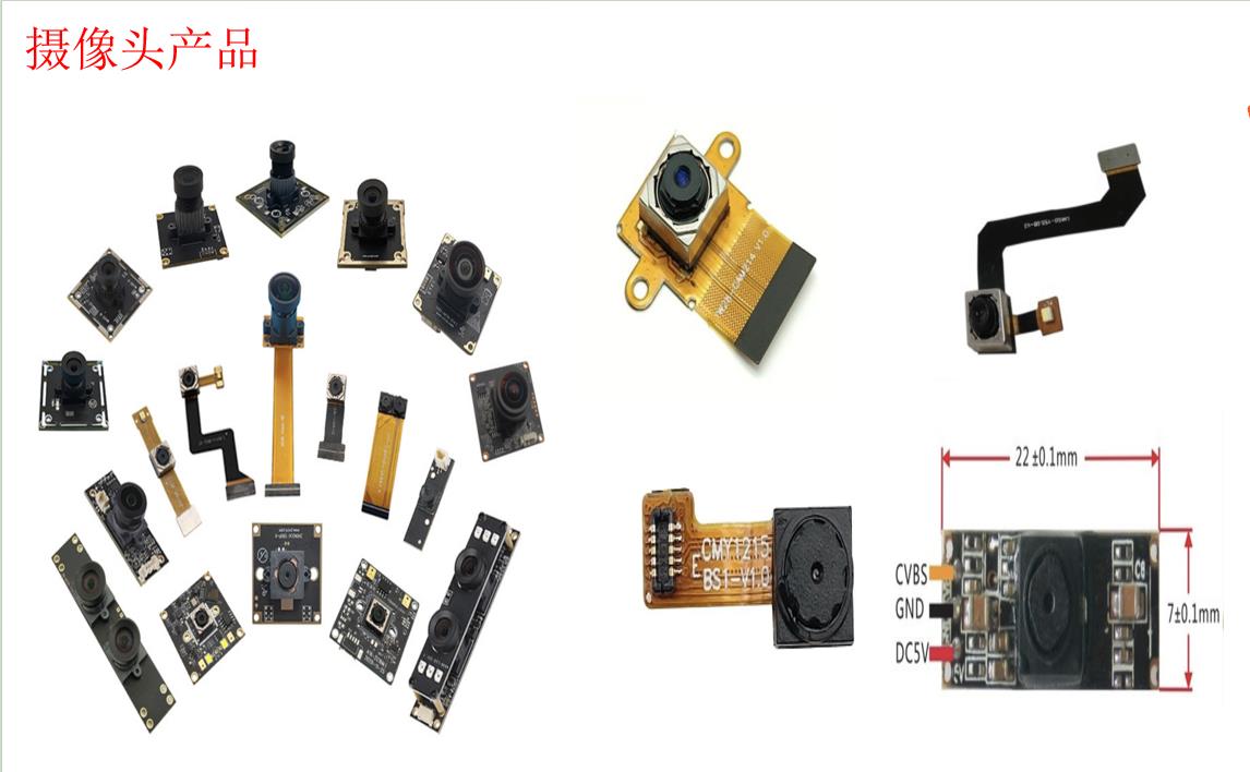 Camera product FPC
Introduction to FPC for camera products Overview o…
Read More
Camera product FPC
Introduction to FPC for camera products Overview o…
Read More
 Backlight plate FPC
Introduction to the FPC of the backlight panel Def…
Read More
Backlight plate FPC
Introduction to the FPC of the backlight panel Def…
Read More
 Eight-layer FPC
Overview of eight-layer laminated board FPC The ei…
Read More
Eight-layer FPC
Overview of eight-layer laminated board FPC The ei…
Read More
 Side key FPC
FPC, which stands for Flexible Printed Circuit Boa…
Read More
Side key FPC
FPC, which stands for Flexible Printed Circuit Boa…
Read More
 Impedance-controlled multilayer FPC
Impedance-controlled FPC is a special type of flex…
Read More
Impedance-controlled multilayer FPC
Impedance-controlled FPC is a special type of flex…
Read More
 3-layer rigid-flex FPC PCB board
PCB type: FPC flexible circuit board Number of lay…
Read More
3-layer rigid-flex FPC PCB board
PCB type: FPC flexible circuit board Number of lay…
Read More
 6-layer Bluetooth headset FPC soft board
PCB type: FPC flexible circuit board Number of lay…
Read More
6-layer Bluetooth headset FPC soft board
PCB type: FPC flexible circuit board Number of lay…
Read More
 Large size thick copper double-sided soft board
Introduction to large-size thick-copper double-sid…
Read More
Large size thick copper double-sided soft board
Introduction to large-size thick-copper double-sid…
Read More
 2-layer fingerprint recognition FPC
Introduction to 2-layer fingerprint recognition FP…
Read More
2-layer fingerprint recognition FPC
Introduction to 2-layer fingerprint recognition FP…
Read More
 Car brake light FPC soft board
Automobile brake light FPC flexible printed circui…
Read More
Car brake light FPC soft board
Automobile brake light FPC flexible printed circui…
Read More
 4 layer LCD display fpc flexible circuit board
PCB type: FPC flexible circuit board Number of lay…
Read More
4 layer LCD display fpc flexible circuit board
PCB type: FPC flexible circuit board Number of lay…
Read More
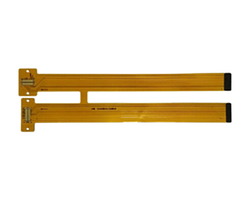 Double-sided FPC ribbon cable
Overview of double-sided FPC cable Double-sided FP…
Read More
Double-sided FPC ribbon cable
Overview of double-sided FPC cable Double-sided FP…
Read More
 Double-sided FPC gold immersion board
Double-sided FPC gold-plated board Double-sided FP…
Read More
Double-sided FPC gold immersion board
Double-sided FPC gold-plated board Double-sided FP…
Read More
 New energy lithium battery FPC protection plate
Overview of FPC protection boards for new energy l…
Read More
New energy lithium battery FPC protection plate
Overview of FPC protection boards for new energy l…
Read More
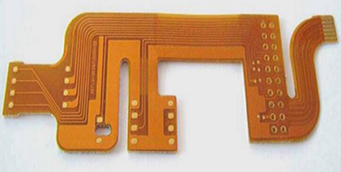
 6-layer FPC circuit board
Introduction to 6-layer FPC circuit boards Product…
Read More
6-layer FPC circuit board
Introduction to 6-layer FPC circuit boards Product…
Read More
 Ordinary single-sided FPC board production and sales
General single-sided FPC boards, namely single-sid…
Read More
Ordinary single-sided FPC board production and sales
General single-sided FPC boards, namely single-sid…
Read More
 Impedance FPC production and sales
Product Overview FPC (Flexible Printed Circuit Boa…
Read More
Impedance FPC production and sales
Product Overview FPC (Flexible Printed Circuit Boa…
Read More
 10-layer rigid-flex FPC HDI board
PCB type: FPC flexible circuit board Number of lay…
Read More
10-layer rigid-flex FPC HDI board
PCB type: FPC flexible circuit board Number of lay…
Read More
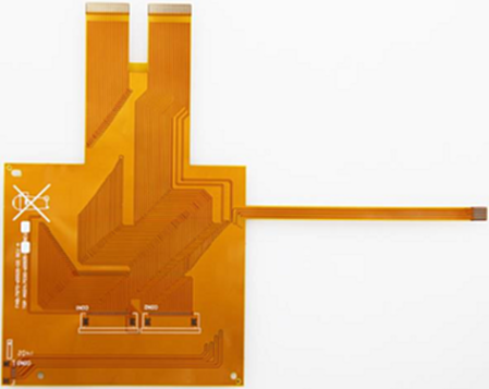
 Medical equipment FPC interface board
PCB type: FPC flexible circuit board Number of lay…
Read More
Medical equipment FPC interface board
PCB type: FPC flexible circuit board Number of lay…
Read More
 Common knowledge of circuit boards: Composition and main functions of some parts of circuit boards
Common knowledge of circuit boards: Composition an…
Read More
Common knowledge of circuit boards: Composition and main functions of some parts of circuit boards
Common knowledge of circuit boards: Composition an…
Read More